1. Introduction
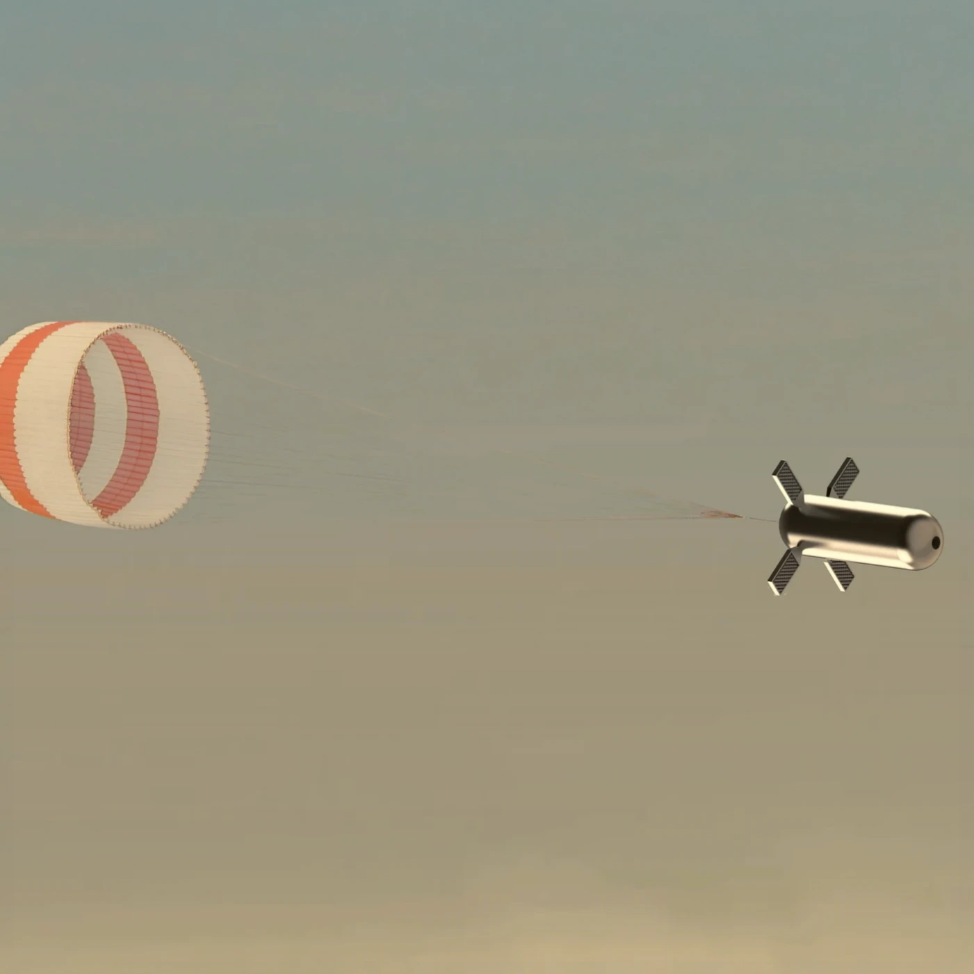
This project was developed as my Bachelor’s Thesis and explored the design of a miniaturised infrared radiometer for future atmospheric missions to Venus, where it would measure the net thermal radiative flux during descent. The objective was to investigate whether modern MEMS technology could be used to dramatically reduce the size, mass and complexity of traditional spacecraft scientific instruments while maintaining their measurement capabilities. The project combined several engineering disciplines, including optics, electronics, MEMS devices, cleanroom fabrication and experimental testing.
The design is based on the DALOMIS Microprobes concept, a mission study published in 2004 by QinetiQ for the European Space Agency. DALOMIS envisioned a balloon drifting through Venus’ atmosphere, releasing over a dozen lightweight microprobes at intervals along its path. Keeping each instrument small was what made carrying so many of them practical, spreading measurements across many locations and times instead of just one. At the time, several of the required technologies, including MEMS devices, were still in their infancy.
Only one instrument has done this before: the Pioneer-Venus Large Probe Infrared Radiometer (LIR), flown in 1978. It remains the only wideband infrared radiometer to have operated inside Venus’ atmosphere. The LIR was, by today’s standards, a bulky and mechanically complex instrument, built around a light pipe geared to a stepper motor. Doing the same job with a micromechanical optical switch is what makes the microprobe concept possible.
2. Instrument Concept
2.1. Scientific Motivation
Venus is often described as Earth’s twin: a rocky planet with 95% of Earth’s diameter and 81.5% of its mass. Its atmosphere, however, sets it dramatically apart.
A dense blanket of cloud reflects around three-quarters of incoming sunlight back into space, making Venus the third-brightest object in the sky as seen from Earth. Despite orbiting 30% closer to the Sun, its atmosphere absorbs an average of 157 W/m², against 240 W/m² for Earth’s.
This atmosphere also traps heat very efficiently once absorbed. The balance between absorbed solar radiation and emitted thermal infrared radiation drives atmospheric circulation, cloud formation and energy transport. How that balance shifts with altitude reveals where the atmosphere is heating and where it is cooling. Measuring how infrared flux varies with altitude therefore lets scientists quantify these processes directly, improving our understanding of Venus’ climate and its unique atmospheric dynamics.
2.2. Wavelengths of Interest
The instrument needed a spectral band wide enough to capture the thermal emission across the whole descent. Planck’s law was applied across the temperatures expected along the way, from around 260 K at the 60 km release altitude to roughly 735 K at the surface. A 3 to 50 μm window, the same band the LIR operated with in 1978, captures 89% of the emitted radiation at 735 K and 95.6% at the coldest.
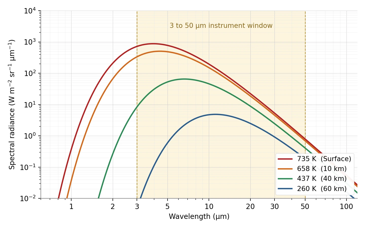
The 735 K figure is a conservative bound, since the probes are not expected to reach the surface: at the 10 km survival limit the window still captures over 93%. Extending the window down to 2 μm would have raised the surface figure to 98.6%, but at the risk of contamination from reflected sunlight, so the lower bound stayed at 3 μm.
2.3. Instrument Architecture
The radiometer concept is built from a minimal set of shared components:
- Two infrared thermopile detectors, one facing zenith and one facing nadir
- A single calibration target
- A MEMS micromirror acting as a shared optical switch
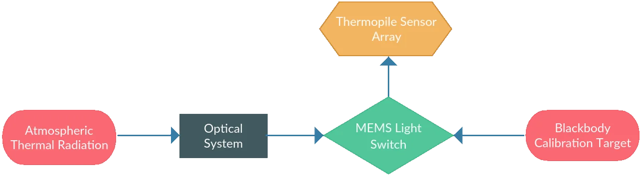
Thermopiles were the natural choice of detector. Bolometers and ferroelectric detectors need cryogenic cooling to work, and the cooling hardware alone would blow the microprobe’s mass budget. Uncooled thermopiles operate reliably across broad temperature ranges, including the 50°C or so expected inside the instrument.
The calibration target exists because the detectors drift as the probe descends and the environment around them heats up. Feeding the sensors a known reference signal at intervals lets that drift be subtracted from the science data. Traditionally this has meant resistively heated blackbody radiators, which need close to 1000 K and carry enough thermal mass that the instrument has to wait for them to warm up and cool down. A micromachined array of silicon filaments does the same job at up to 1200 K, on a few watts, with warm-up and cool-down times measured in milliseconds.
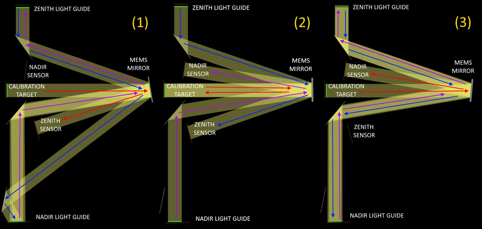
Measuring net thermal flux requires observing the upward and downward radiation simultaneously, since net flux is defined as the difference between the two. Duplicating the mirror and calibration target for each direction would have simplified the layout, but at the cost of extra components and extra mass. A single mirror and calibration target are therefore shared between both sensors.
In its relaxed position, the mirror reflects the zenith and nadir light guides straight into their respective detectors, allowing simultaneous remote sensing in both directions. To calibrate either sensor, the mirror tilts instead to steer the calibration target’s signal into it. This gives the instrument three operating modes:
- Zenith sensor calibration (1)
- Remote sensing in both directions at once (2)
- Nadir sensor calibration (3)
3. MEMS Micromirror Selection
3.1. Trade-off Between MEMS Technologies
The success of the instrument depended heavily on selecting an appropriate MEMS mirror. Several commercially available technologies were investigated, including electrostatic, piezoelectric and electromagnetic devices. Each presented advantages and disadvantages in terms of power consumption, control complexity, achievable angular range and linearity.
Electrostatic mirrors offered low power consumption but required high driving voltages and exhibited non-linear behaviour. Piezoelectric mirrors provided compact designs but suffered from hysteresis and limited angular deflection. Electromagnetic mirrors, while somewhat larger and more power-hungry, provided a highly linear relationship between drive current and mirror angle, greatly simplifying control. They also allowed a wider deflection range in point-to-point operation, up to ±15° compared to around ±5° for electrostatic devices, giving more flexibility when designing the optical layout.
3.2. Hamamatsu S12237-03P
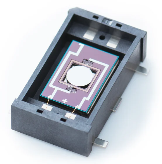
After evaluating the available options, the Hamamatsu S12237-03P was selected. This device uses electromagnetic actuation to achieve optical deflections of approximately ±15°. The mirror, 2.6 mm across, incorporates a miniature coil suspended on torsion springs and surrounded by a magnetic field generated by an internal permanent magnet. By varying the current flowing through the coil, the mirror can be tilted precisely and predictably.
One of the key advantages of this device was its near-perfect linear response of approximately 1° of optical deflection per milliampere of current. This characteristic made it ideal for point-to-point optical switching applications such as the radiometer concept developed in this project. Despite the generally higher power demands of electromagnetic actuation noted above, this specific device draws no more than 37.5 mW at maximum deflection, a modest figure given the microprobe’s strict power constraints.
4. Driver Electronics Design
4.1. Current Source Design
The mirror angle follows the coil current, but the coil’s resistance does not stay constant. This unit measured 159 Ω at 25°C, and resistance climbs roughly linearly with temperature, at about a third of a percent per degree. Across the −20 to 70°C range the device is rated for, that adds up to a swing of about ±15%, pushed both by the surrounding environment and by the coil dissipating its own power. Under a fixed supply voltage the current, and with it the mirror angle, would drift with temperature. Regulating the current directly removes the problem at its source.
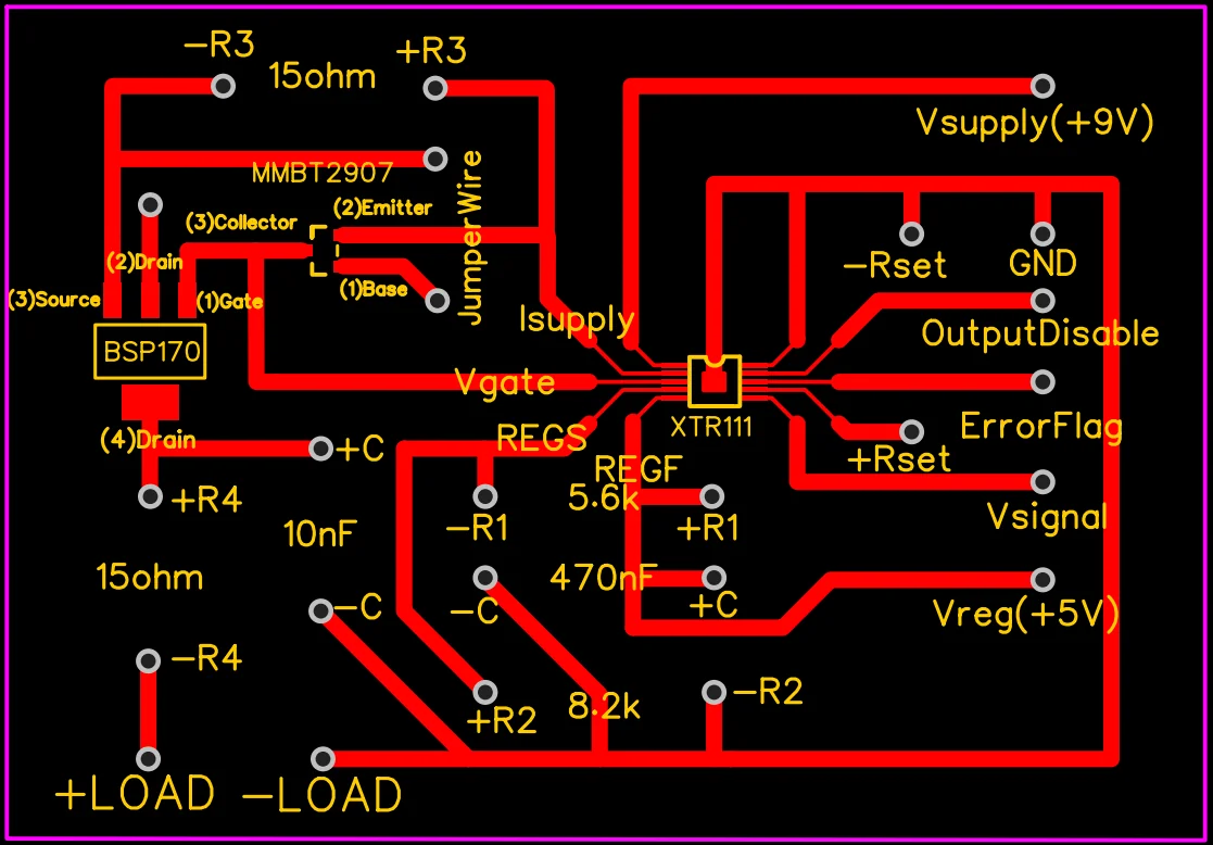
A dedicated current source PCB was developed around the Texas Instruments XTR111 precision voltage-to-current converter IC. This device allowed a low-voltage control signal to generate controlled coil currents across the full operating range of the mirror. The design also incorporated protection circuitry to prevent accidental overcurrent conditions, as well as a precision voltage regulator capable of supplying stable reference voltages to other components within the system.
The assembled board was then verified against its specification, with the output current measured across the full 0 to 5 V input range. The response was linear throughout and matched the theoretical transfer function.
4.2. H-Bridge
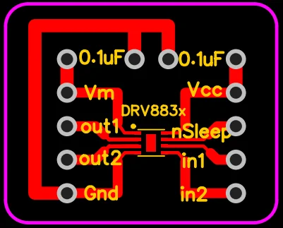
To enable bidirectional mirror motion, a DRV8838 H-Bridge IC was incorporated into the design. This made it possible to reverse the direction of current flow through the mirror coil, allowing the mirror to tilt both positively and negatively. The output current was measured in both directions and fitted to a linear expression for each, so that any offset between the commanded and delivered current could be corrected in the control code.
4.3. DAC
An MCP4725 digital-to-analogue converter generated the control voltage driving the current source. Twelve bits of resolution were more than sufficient here. Each of its 4096 discrete steps corresponds to a current change of roughly 0.0037 mA at the coil, or about 0.0037° of optical deflection. That is some two orders of magnitude finer than the mirror’s own repeatability, so a higher resolution would only have added cost.
The MCP4725 also communicated over I²C, which kept the control code simple. Its 5 V reference came from the XTR111’s own voltage regulator, which held it clean and stable without adding another supply.
4.4. MEMS Mirror
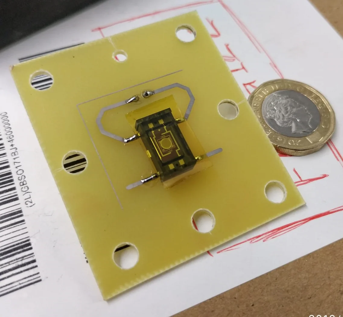
To physically support the MEMS mirror and mechanically interface with the experimental set-up, a custom PCB was also designed and manufactured. Soldering the mirror onto it was tricky. The datasheet allowed no more than 260°C and ten seconds per joint, and the permanent magnet inside kept dragging the device onto the tools. The fix was to rest the PCB on a heavy iron slab, which held the mirror magnetically in place while it was soldered.
4.5. Assembly of the Control System
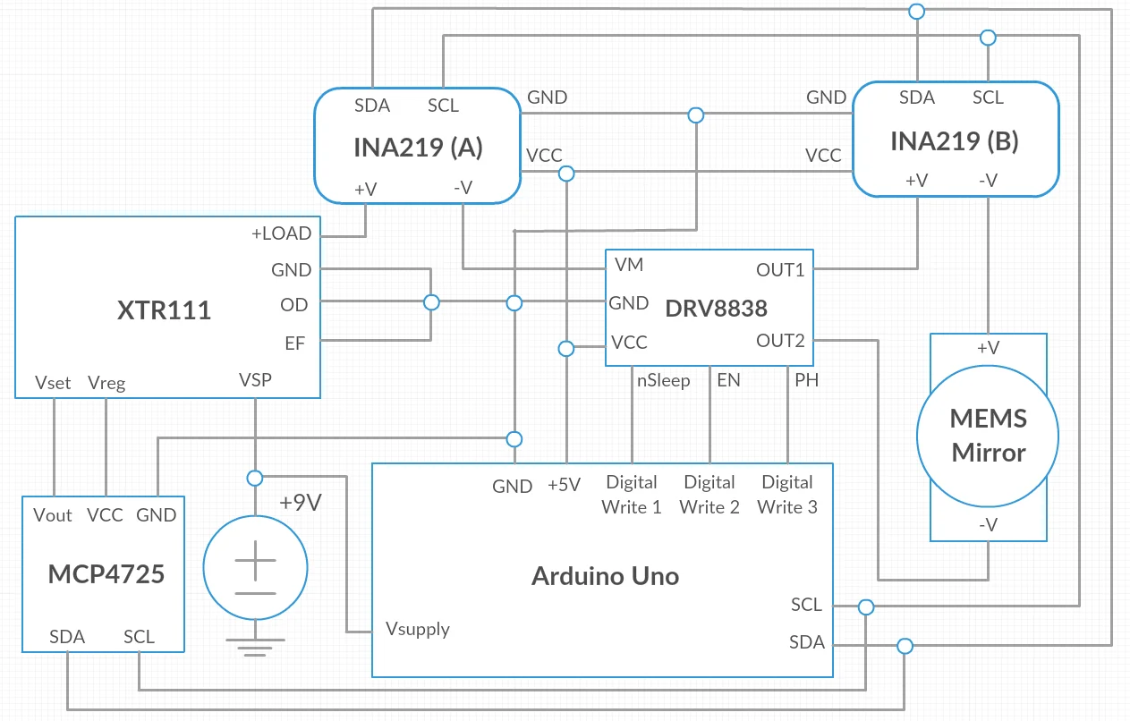
The complete control system consisted of:
- MEMS mirror + custom-designed PCB
- XTR111 current source IC + custom-designed PCB
- DRV8838 H-Bridge IC + custom-designed PCB
- MCP4725 DAC
- Arduino Uno microcontroller
- INA219 current monitoring sensors
The software developed to run on the Arduino allowed precise angle control of the mirror, as well as dynamic motion profiles such as sinusoidal scanning patterns.
5. Infrared Optimisation Through Gold Coating
5.1. Coating Selection
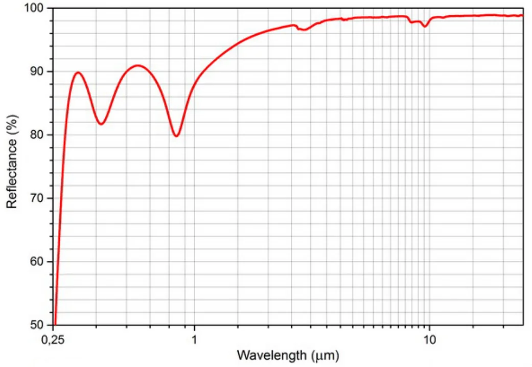
The selected mirror was supplied with a protected aluminium coating, but the instrument had to perform across the full 3 to 50 μm window. What mattered most was the 8 to 15 μm band, the region of greatest scientific interest. Aluminium, silver and gold were all evaluated as alternatives.
On optical grounds silver was the early favourite, reflecting around 98% across the infrared. What ruled it out was its surface chemistry. It reacts with sulphides to form a tarnish that eats into that reflectance. The mirror would have had to be handled in a sealed inert environment, and then carry a protective dielectric layer for the rest of its service life. That is a great deal of complexity to design into a microprobe.
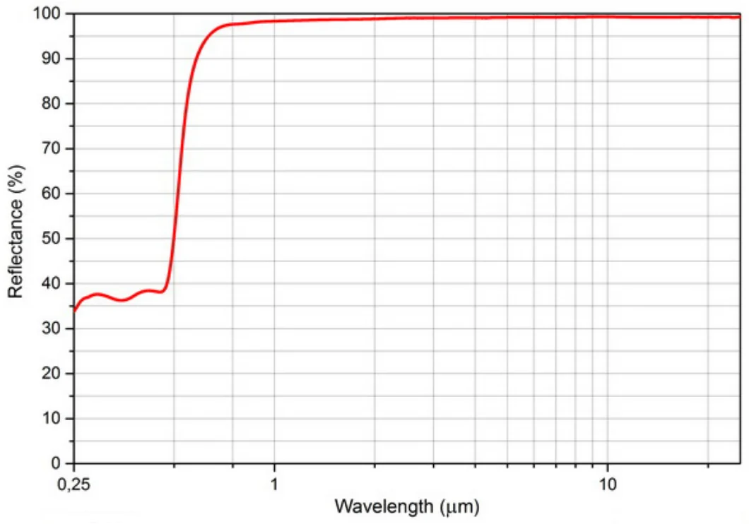
Gold was selected instead. Its reflectance stays above 97% from 1000 nm upwards and it does not react with the atmosphere at all under normal conditions. Within the 8 to 15 μm band it also edges out aluminium, which made it the better choice here. Aluminium remains the more versatile coating overall, holding up from the ultraviolet through to the far infrared, whereas gold’s reflectivity collapses to around 35% below 600 nm.
Since gold is a soft metal and prone to mechanical damage, a protective silicon oxide layer is often added. It was left out here for the same reason that counted against silver: the extra layer introduces absorption bands inside the instrument’s operating range.
Optical calculations based on the skin depth of gold, around 32 nm at the longest wavelength of interest (50 μm), showed that just a few multiples of this thickness would make the mirror effectively opaque. Three skin depths alone, for instance, already bring transmittance under a quarter of a percent.
Since the relationship is exponential, transmittance can never reach zero, so the thickness had to be a compromise. To anchor the choice, the coatings used on mirrors already optimised for the infrared were consulted. The James Webb Space Telescope was the natural reference, its beryllium mirrors carrying a 100 nm gold layer for the mid to far infrared. At 50 μm, 100 nm works out to 3.11 skin depths, which puts transmittance at roughly 0.19%. A final thickness of 100 nm was therefore adopted.
5.2. Physical Vapour Deposition (PVD)
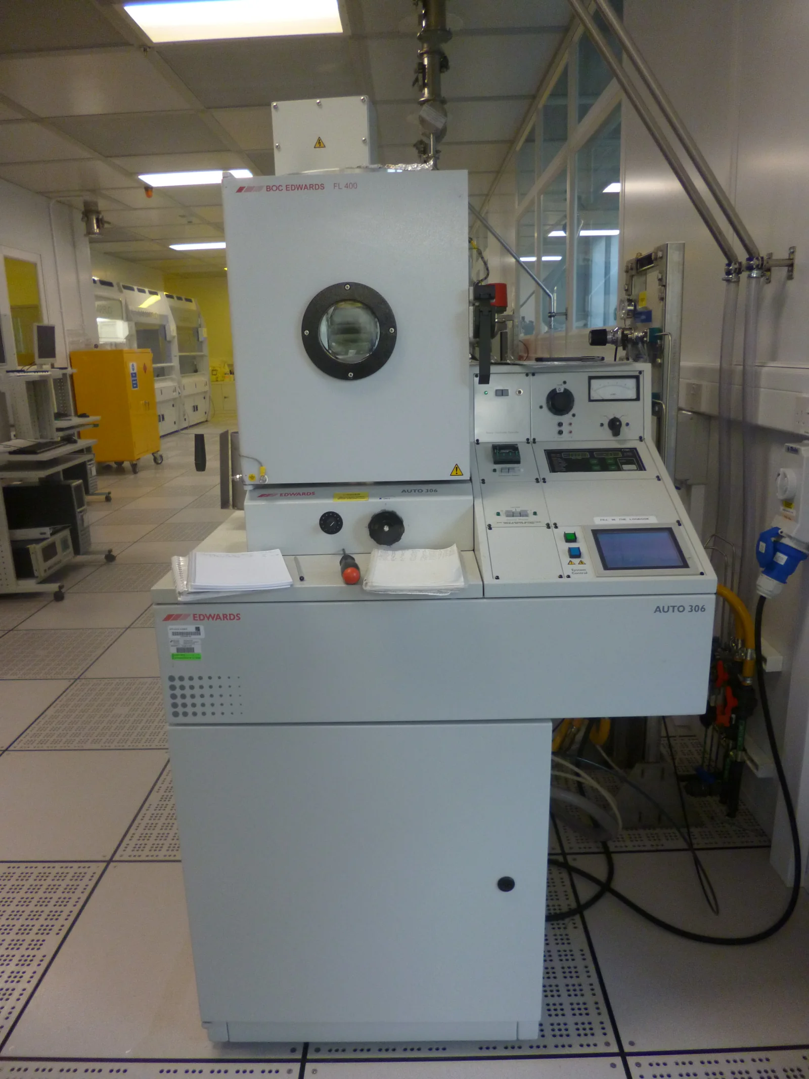
Applying the coating was one of the most challenging aspects of the project. Since the manufacturer could not provide custom-coated mirrors individually, the coating had to be performed manually using Physical Vapour Deposition (PVD).
The mirror was first taken to the cleanroom to be inspected up close and to work out a coating strategy. Three concerns came out of that inspection:
- Any gold landing on the coil would bridge adjacent turns, reducing the effective turn count and flattening the mirror’s deflection curve, so everything except the mirror surface itself had to be covered.
- The device might fail during evacuation if air were trapped anywhere inside it. The manufacturer had no data on how the part behaves under vacuum and could not rule the possibility out, though they thought it unlikely. The risk was accepted.
- Prolonged heat inside the chamber risked demagnetising the tiny permanent magnet, which set an upper bound on the deposition rate.
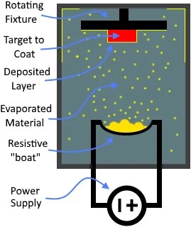
Two main PVD methods were considered: sputtering, which ejects atoms from a gold sample using energetic ions, and thermal evaporation, which vaporises the gold by heating it. Sputtering was ruled out because the energetic particles it produces would heat the device well past what the magnet can tolerate. Resistive evaporation, a form of thermal evaporation where the gold is heated directly by passing a current through it, was chosen instead for its gentler, more controllable heating.
The mask was made by laying a 2 mm washer over a strip of Kapton tape and drilling through it, which left a reasonably clean circular aperture. Kapton was chosen because it is stiff enough to drill, does not outgas noticeably under vacuum, and insulates the device from some of the heat during deposition. Coating only 2 mm of the 2.6 mm mirror was deliberate, keeping the gold well clear of the edges.
Once masked, the mirror was mounted onto the evaporator’s rotating plate, facing the resistive boat loaded with the gold pellets below. The chamber was then sealed and evacuated to a high vacuum of around 5×10⁻⁷ mbar using a turbopump cooled with liquid nitrogen. This took about an hour, after which the deposition could begin.
The deposition rate was held at about 0.1 nm/s, slow enough to keep the temperature sensor on the plate below 60°C, the safe limit for the mirror. It was tracked in real time using a quartz sensor inside the chamber, which measured the total thickness deposited from its own vibration frequency. Gold was gradually evaporated until the desired thickness of 100 nm had been deposited.
5.3. Post-Coating Inspection
Following deposition, the device was inspected under a microscope. The film itself was very homogeneous and closely matched the intended geometry. A few flakes of debris had settled on the surface, most likely left over from earlier depositions inside the chamber.
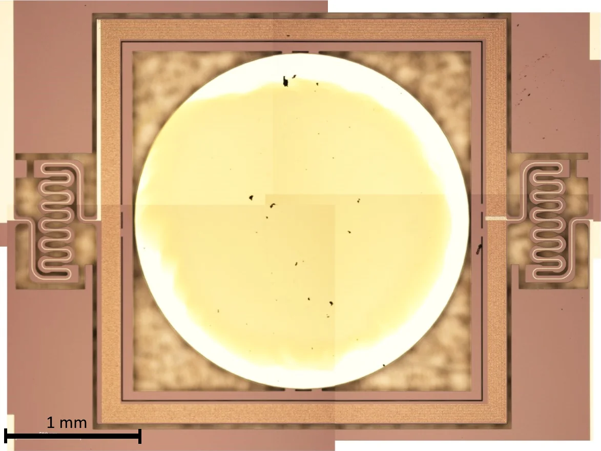
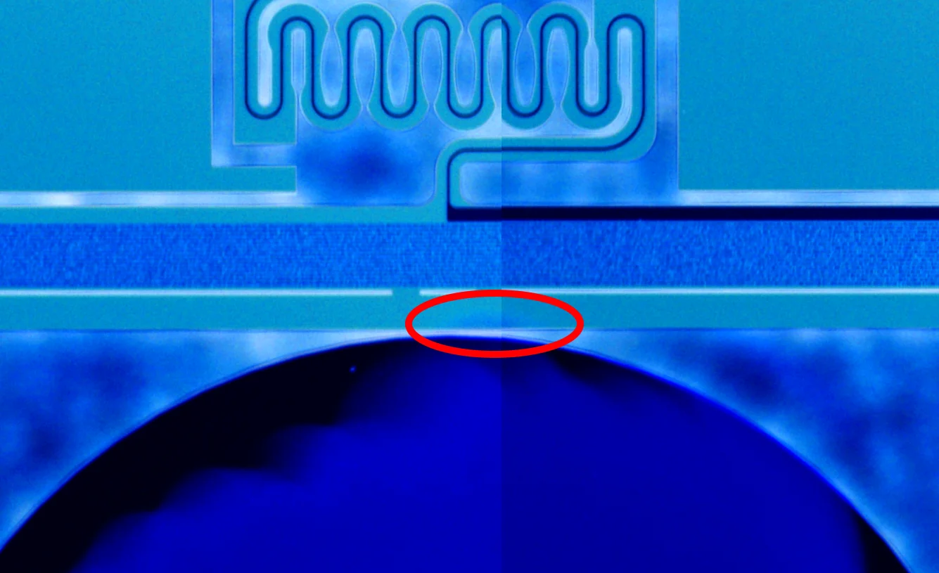
No gold had reached the coils, but a faint layer had crept onto the support frame uncomfortably close to them, so the masking still had room for improvement.
6. Optical Test Rig Development
Every unit deviates slightly from the datasheet’s ideal 1°/mA. Most of the spread comes from variation in the strength of the individual permanent magnets, with imperfections in the torsion bar contributing a little non-linearity of their own. Each device therefore has to be characterised individually, and in this case the characterisation doubled as a check that the coating process had not altered anything.
6.1. Design and Manufacturing
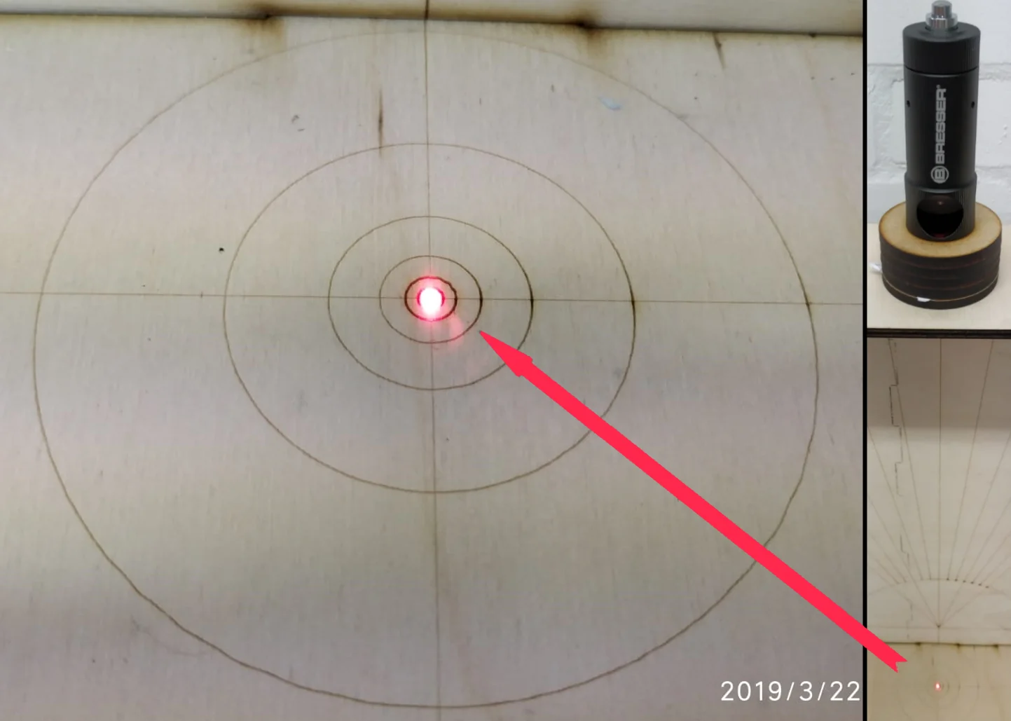
A dedicated optical test rig was devised for the purpose, consisting of a laser source, a calibrated angular measurement scale and an adjustable mounting mechanism for the MEMS mirror.
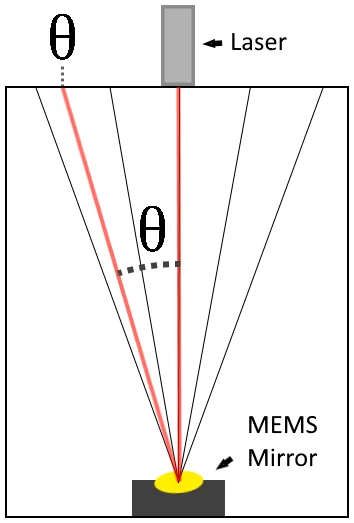
The rig was first developed in CAD software and then fabricated using laser-cut components, giving a stable and repeatable environment for optical testing.
6.2. Test Methodology
Testing was carried out by directing a collimated laser beam onto the mirror surface and observing the reflected beam position on a calibrated scale. By varying the supplied coil current, the corresponding mirror angle could be measured directly. The current itself was read with one of the INA219 sensors, whose 0.1 mA resolution put the instrumentation uncertainty at ±0.05 mA. Repeated measurements were performed in both directions of rotation to assess repeatability and linearity.
7. Experimental Results
7.1. Mirror Characterisation
The experimental testing showed that the mirror exhibited an almost perfectly linear relationship between coil current and optical deflection angle, with every fit returning an R² of 0.999 or better. Each direction was measured twice.
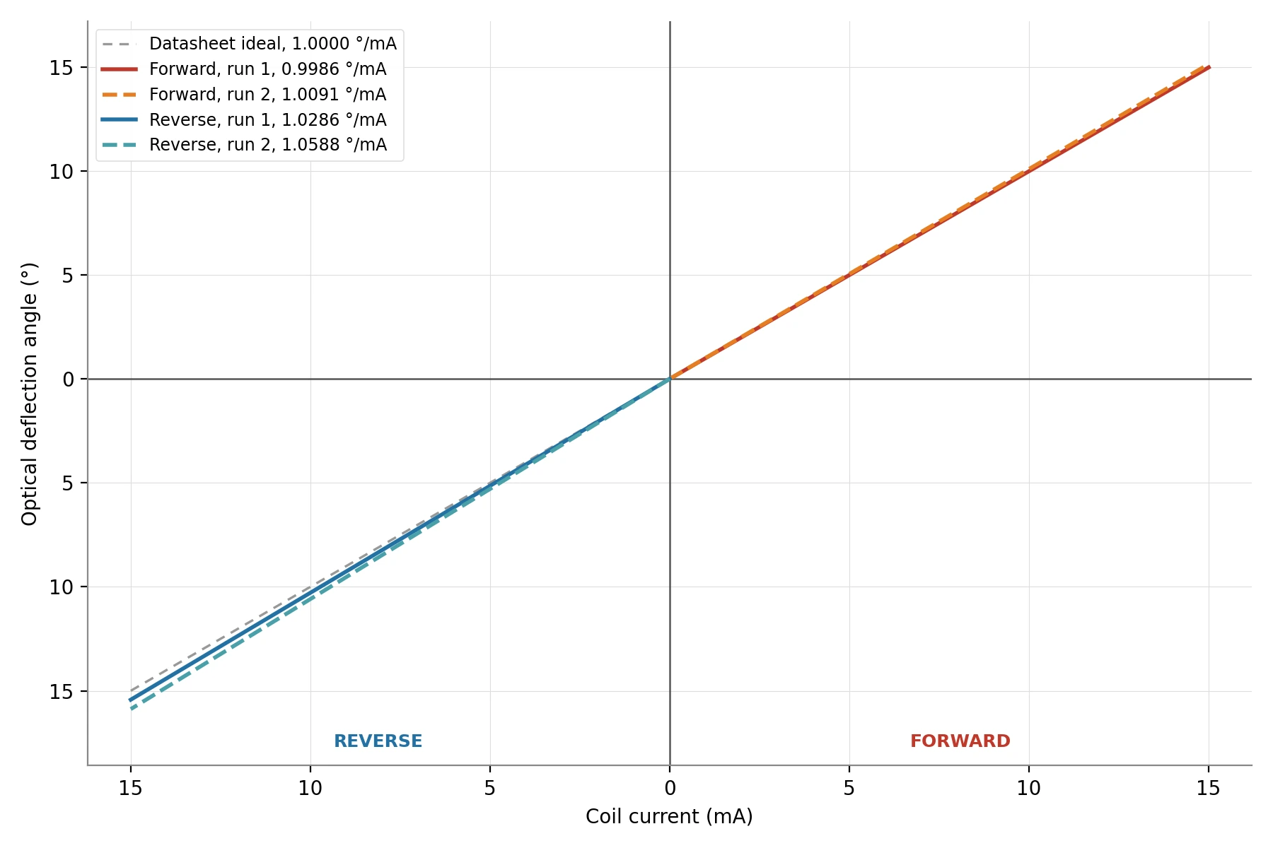
The forward runs tracked the ideal almost exactly, averaging 1.0038 °/mA, while the reverse runs came out slightly steeper at 1.0437 °/mA. Both sit well inside the datasheet’s ±10% tolerance.
The repeat runs also diverged more as the deflection angle grew, reaching a worst case of 0.25° in the forward direction and 0.46° in the reverse. That pattern points to the mirror shifting slightly in its mount during the test rather than to any behaviour of the device itself.
Taken together, these results confirmed the mirror’s suitability for precision optical switching.
7.2. Performance Validation
Perhaps the most important result was that the mirror continued to operate normally after the gold-coating process, with no measurable degradation from the vacuum or the heat. A commercially available MEMS device can therefore survive the manufacturing steps needed to adapt it for infrared scientific measurements.
8. Infrared Reflection Demonstration
8.1. Experimental Set-up
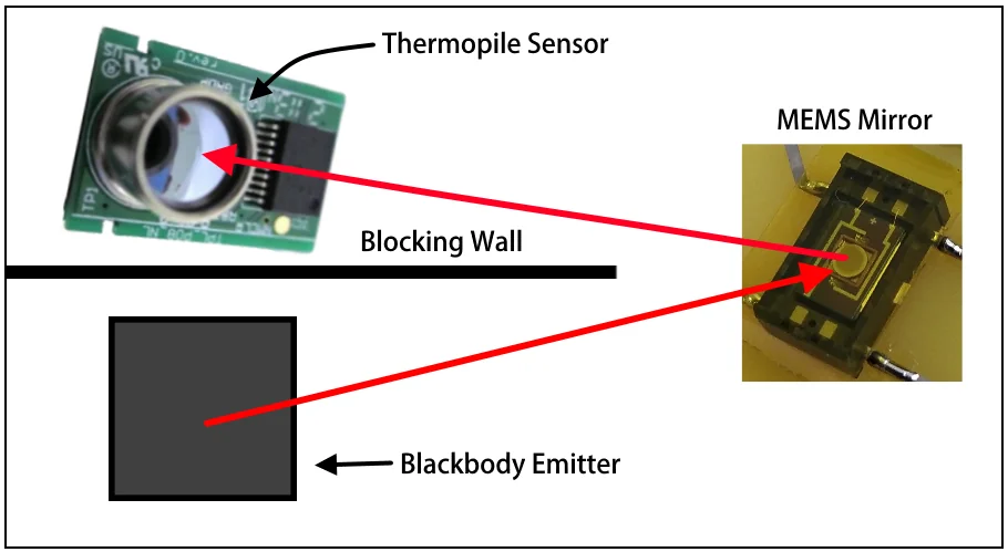
As a final validation exercise, the gold-coated MEMS mirror was tested in a joint experiment with another student, whose own project focused on characterising the thermopile sensor. The test brought both halves of the instrument concept together for the first time, and its purpose was to verify that the mirror could effectively redirect thermal infrared radiation towards the detector.
The blackbody source was resistively heated to approximately 90°C, with the mirror 3 cm in front of it and the thermopile a further 3 cm from the mirror. A wall between the emitter and the sensor kept thermal crosstalk out of the measurement, and the thermopile was fitted with a filter passing only 5.5 to 13.5 μm.
8.2. Results and Discussion
The experiment confirmed that the mirror could redirect thermal infrared radiation as required by the radiometer architecture.
The thermopile read 65°C through the mirror. Its noise reduction filter attenuated the signal to 85.6%, which brought the figure to 75.9°C, and correcting for the mirror’s nominal reflectivity across this narrower band, around 99%, gave 76.7°C. Placed directly in front of the emitter the same sensor read 90°C, matching the thermistor on the blackbody itself. Reflected off the mirror, then, the measurement fell 14.7% short of the true value.
The exact source of this disparity is not fully clear. Condensation on the mirror surface is one likely explanation, since relative humidity was high on the day of the experiment and water is a strong absorber of infrared radiation. A small misalignment between the mirror and the thermopile, picking up some signal from the surrounding PCB rather than the mirror itself, could also account for part of the gap. The noise reduction figure is itself only an average and shifts somewhat with signal strength, so part of the gap may be an artefact of the correction rather than a real loss at the mirror.
Further research would be needed to isolate the actual cause, but the experiment still connected the work on MEMS actuation, infrared optics and detector technology into a complete system-level demonstration.
9. Conclusions
This project successfully demonstrated the feasibility of using a commercially available electromagnetic MEMS micromirror as an optical switching element within a miniaturised infrared radiometer concept. It also strengthened the wider case for the technology in compact planetary instruments. The work involved the complete development cycle of a scientific instrumentation subsystem, including component trade studies, electronics design, PCB development, microcontroller programming, cleanroom fabrication processes, optical testing and experimental validation.
Of the two thermal effects on the device, only one was fully resolved. Driving the mirror from a current source holds the deflection angle steady despite the coil’s changing resistance. The second, the weakening of the permanent magnet, was characterised on paper and a correction derived from the coil resistance, but implementing it in the control loop was left for future work. Surviving the PVD chamber also validated the device against something it was never deliberately tested for: the relatively hot conditions, up to 50°C, expected inside the microprobe during atmospheric descent.
Several avenues remain open for future development of the concept. Acoustic testing of the mirror’s torsion beams would be an important piece of qualification work, since the manufacturer has no data on how the device withstands the environment of a launch. The theoretical reflectance of the gold coating was calculated but never experimentally verified, so measuring it directly would help confirm the predicted optical performance.
Finally, the natural next step would be to build a complete prototype of the instrument, combining both sensors, the shared mirror and calibration target. Its performance could then be tested across the full range of ambient conditions expected during descent through Venus’ atmosphere.